LX2202
2A Li-Ion Linear Charger and Power Control
®
TM
P RODUCTION D ATA S HEET
KEY FEATURES
DESCRIPTION
The LX2202 (compared to the LX2201)
has improved charge and discharge mode
detection circuitry. A UVLO feature prevents
battery charging when VDD is less than 3.6V.
The LX2202 uses three resistors to
program the constant charge current level, for
setting the termination charge current, and for
varying the USB charge current limits.
LX2202 support two types of Li-Ion
battery chemistry; 4.1V and 4.2V through
logical input (VM pin). The LX2202
provides a charging status indicator.
The LX2202 features a pre-charge
conditioning mode for batteries that have
been deeply discharged and also has a top off
charge mode for batteries that are left on the
charger for extended periods.
The LX2202 is available in a high power
4mm x 4mm, 20-pin MLP, surface mount
package.
Up to 2A Charge Current
Internal Pass Element Can
Function as a Reverse Direction
Load Switch
USB Compliant Charging States
using optional USB input
Isolated Battery Topology
Low RdsON in Discharge Mode
Full Capacity Charging
True Charge Indicator
Wall Supply Regulator Tolerance
5V + 10%
Topping Charge with Voltage
Monitoring Mode
Improved charge/discharge mode
detection circuitry
Small, High Power 20-lead MLP
package
Selectable Li-Ion Battery for 4.1V
or 4.2V Applications
WWW . Microsemi .C OM
The LX2202 Linear Battery Charger is a
multi-state (2 stage) Li-Ion battery charger
(Constant current / Constant voltage) that is
designed to minimize battery charge time
(even from current limited sources such as
USB) and provide a simplified interface to
control battery discharge.
LX2202 features up to 2A charging
current from an AC adapter and an isolated
battery topology to minimize charge time
from current limited sources such as USB.
A thermal control loop maintains a safe
operating temperature at all times.
The LX2202 provides a seamless
complete battery interface. When the input
power source is removed, the LX2202
provides the discharge path for the battery
with extremely low discharge impedance.
This eliminates the need for external
discharge switch and voltage supervisors.
In USB mode, the LX2202 provides
three levels of current limit: 100mA,
500mA, and off.
APPLICATIONS
Batteries up to 4AH Ratings (C/2)
Cell Phones
PDAs
Charging Cradles
Digital Cameras
Low Cost Single Li-Ion Cell Chargers
IMPORTANT: For the most current data, consult MICROSEMI’s website: http://www.microsemi.com
Patent Pending
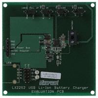
PRODUCT HIGHLIGHT
State Select Truth Table
Power On/Off
NU
PSW
VID1
VDD
VID0
VM
Main Internal
Power Bus
NU
VDD
LX2202
BAT
VDD
BAT
0
0
0
1
1
0
Charging – USB low level if
using USB.
1
1
Charging – USB high level if
using USB.
10µF
CMP
CCP
CTP
STAT
CUS
GND
USB
0.1µF
10µF
VID1
BAT
VDD
B220
Wall Adapter
VID0
2.55k
105k
72.3k
To VDD
Charge
Indicator
2.49k
VDD > VBAT
Switch open – charging
disabled.
Charging – USB high level if
using USB.
VBAT > VDD
Switch open – discharge
disabled.
Switch open – discharge
disabled.
Battery Discharging. MOSFET
fully enhanced with current
flow VBAT to VDD.
Battery Discharging. MOSFET
fully enhanced with current
flow VBAT to VDD.
PACKAGE ORDER INFO
LQ
Plastic MLP
4x4mm 20-Pin
RoHS Compliant / Pb-free
-40 to 125
Copyright © 2004
Rev. 1.0a, 2006-02-09
Note: Available in Tape & Reel.
Append the letters “TR” to the part number.
(i.e. LX2202CLQ-TR)
LX2202
TA(°C)
LX2202CLQ
Microsemi
Integrated Products Division
11861 Western Avenue, Garden Grove, CA. 92841, 714-898-8121, Fax: 714-893-2570
Page 1
�LX2202
2A Li-Ion Linear Charger and Power Control
®
TM
P RODUCTION D ATA S HEET
VID0
VID1
PSW
NU
20
19
18
17
16
VDD
1
15
NU
VDD
2
14
BAT
VDD
3
13
BAT
VDD
4
12
BAT
USB
5
11
CMP
8
9
10
STAT
CCP
Note: Exceeding these ratings could cause damage to the device. All voltages are with respect to
Ground. Currents are positive into, negative out of specified terminal.
7
CTP
6
CUS
Pad Is GND
WWW . Microsemi .C OM
Supply Voltage (VUSB or VDD ) ..........................................................-0.3V to 7V
Analog Input Signals (VIDx, VM, SNS) .............................................-0.3V to 7V
Battery Charging Current (IBAT).........................................................................2A
Discharge Current (IVDD)....................................................................................3A
Operating Junction Temperature.................................................................. 150°C
Storage Temperature Range...........................................................-65°C to 150°C
USB Maximum DC Current .......................................................................500mA
USB Maximum Surge Current...........................................................................2A
RoHS / Pb-free Peak Package Solder Reflow Temperature
(40 second maximum exposure) ...................................................... 260°C(+0, -5)
VM
PACKAGE PIN OUT
GND
ABSOLUTE MAXIMUM RATINGS
LQ PACKAGE
(Top View)
THERMAL DATA
RoHS / Pb-free 100% Matte Tin Lead Finish
LQ
Plastic Micro Lead Frame Quad Package 20-Pin
THERMAL RESISTANCE-JUNCTION TO AMBIENT, θJA
40°C/W
Junction Temperature Calculation: TJ = TA + (PD x θJA).
The θJA numbers are guidelines for the thermal performance of the device/pc-board system. All of the
above assume no ambient airflow.
FUNCTIONAL PIN DESCRIPTION
Name
Description
BAT
Charging Output - This pin is wired to the positive terminal of the battery. (The negative battery terminal is wired to GND.)
CCP
Charge Current Programming Pin - A resistor (RCP) is connected between this pin and GND. The constant current is
determined by the following relationship:
73200
CMP
Compensation Pin – Connect a 0.1µF compensation capacitor from this pin to VDD.
CTP
Charge Termination Programming Pin – A resistor (RTP) is connected between this pin and GND. The termination charge
current is determined by the following relationship:
5250
CUS
GND
PSW
R CCP
I BAT( MIN) =
R CTP
Maximum USB Current Programming Pin – A resistor (RUS) is connected between this pin and GND. The Hi Level charge
current is determined by the following relationship:
1211
I USB( HIGH) =
R USB
Common Ground
This pin is floating and will not affect performance.
PMOS Switch driver – This output is designed to drive the gate of an external PMOS power switch. The driver is pulled low
(PMOS on state) when VDD > VBAT.
VDD
Common Power Node – Connects to system power bus.
VIDx
State Select Input – Applying a two bit TTL compatible signal sets the desired state of the charger corresponding to the Truth
Table.
USB
Voltage Input – Current limited USB input. Apply a USB compliant power input.
VM
STAT
Voltage Mode Select - Selects the constant voltage charge level. Wired to USB for 4.1V and GND for 4.2V.
Status - This pin is a logic high level when the battery is being charged. A low signal indicates either under voltage lockout,
charge completed, or VBAT > VDD, or VID0 = VID1 = 0.
Copyright © 2004
Rev. 1.0a, 2006-02-09
Microsemi
Integrated Products Division
11861 Western Avenue, Garden Grove, CA. 92841, 714-898-8121, Fax: 714-893-2570
Page 2
PACKAGE DATA
NU
I BAT( MAX) =
�LX2202
®
TM
2A Li-Ion Linear Charger and Power Control
P RODUCTION D ATA S HEET
ELECTRICAL CHARACTERISTICS
`
`
`
Parameter
Symbol
MAIN CIRCUITRY
Input Voltage
USB Input voltage
Under Voltage Charging Lockout
VDD
VUSB
VDDUVLO
Quiescent Current
IGND
CTP Bias Voltage
CCP Bias Voltage
CUS Bias Voltage
CONSTANT VOLTAGE MODE
VCTP
VCCP
VCUS
Constant Voltage Charge Voltage
VCVL
Top Off Charge Droop Threshold
CONSTANT CURRENT MODE
BAT Constant Current Accuracy
Conditioning Current
`
`
`
`
`
ICCL
0.85
1
1.15
VVID
VM = Lo; -40C to 125C
VM = Hi; -40 to 125C
3.60
2.1
20
9
1.26
1.26
2.6
VDRP
State Select Threshold
VBAT < VCTV ; @25°C
3.0
4.6
6.0
2.8
VCTV
V
V
V
mA
µA
µA
V
V
V
V
%
VBAT
VCVL
A
%
IBAT
ICCL
V
IBAT
@25°C
35
50
65
mA
IIN
IIN
VUSB = 5V, VDD < VUSB, VID1 = Lo
VUSB = 5V, VDD < VUSB, VID1 = Hi
85
425
93
463
100
500
mA
mA
4.5
5
0.4
V
V
VVM
THERMAL SHUTDOWN
Maximum Junction Temperature
TJ
BI-DIRECTIONAL PASS ELEMENT CONTROL
Discharge Switch On Resistance
RDS(ON)
Charging Threshold
VCHG
Discharging Threshold
VDCH
Pass Element Switch Mode Delay
tsw
PSW FET DRIVER
High Output Voltage
VPSW
Low Output Voltage
VPSW
ORing Resistance
RPSW
Switch Delay (after tsw)
tPSW
HEAD ROOM
Copyright © 2004
Rev. 1.0a, 2006-02-09
VBAT = 0; Rising VDD
VDD > VBAT
VDD < VBAT
VDD < VBAT, VID0 = VID1 = 0V
IBAT > 100mA
Units
6
6
3.85
4
40
15
4.24
4.14
98
VSTAT
VSTAT
Discharging headroom
4.5
4.35
Max
4.2
4.1
97
Conditioning Current Mode
Threshold Voltage
Charge Termination Current
Accuracy
USB CURRENT LIMIT
USB Low Current Limit
USB High Current Limit
LOGIC
STAT Logic High Output
STAT Logic Low Output
Charging headroom
LX2202
Typ
VUSB = 5.0V, ISTAT = -5mA
VUSB = 5.0V, ISTAT = 25µA
Logic Hi
Logic Lo
Logic Hi
Logic Lo
VUSB = 5.0V, IOUT = 1A, Temperature Rising
2.0
0.8
2.0
0.8
130
IBAT = -1A (Not Tested)
VUSB > VBAT + VCHG
VUSB < VBAT + VDCH
Charge–to–discharge or Discharge–to–charge
VUSB < VBAT, IPSW = 0, VBAT = 4.2V
VUSB > VBAT, IPSW = 0
CPSW = 1000pF, to VPSW = (VBAT – 1V)
4.1
5
0
VDD – VBAT, IBATT = 5mA; not tested in
production
VBAT – VDD, IBATT = -20mA; not tested in
production
Microsemi
Integrated Products Division
11861 Western Avenue, Garden Grove, CA. 92841, 714-898-8121, Fax: 714-893-2570
V
V
140
150
°C
130
40
60
5
150
10
mΩ
mV
mV
µs
0.2
15
1000
V
V
KΩ
Ns
4.2
0
10
500
65
mV
65
mV
ELECTRICALS
`
Min
4.16
4.06
96
ICOND
VM Select Threshold
Test Conditions
WWW . Microsemi .C OM
Unless otherwise specified, the following specifications apply over the ambient temperature 0°C ≤ TA ≤ 70°C except where otherwise
noted and the following test conditions: VDD = 5.0V, VM = GND, VID0 = VID1 = VBAT, RCCP = 72.3k, RCTP = 105k, RUSB =
2.55k.
Page 3
�LX2202
®
TM
2A Li-Ion Linear Charger and Power Control
P RODUCTION D ATA S HEET
SIMPLIFIED BLOCK DIAGRAM
WWW . Microsemi .C OM
UVLO
VID0
PSW
VDD
USB
STAT
CHARGE/
DISCHARGE
CONTROL
0.1
BAT
CHARGE
TERMINATION
CONTROL
CUS
VID1
VM
CTP
USB
LIMIT
CONTROL
CONSTANT
VOLTAGE
CONTROL
CMP
TEMPERATURE
CONTROL
CCP
CONSTANT
CURRENT
CONTROL
GND
Figure 1 – Simplified Block Diagram
BLOCK DIAGRAM
Copyright © 2004
Rev. 1.0a, 2006-02-09
Microsemi
Integrated Products Division
11861 Western Avenue, Garden Grove, CA. 92841, 714-898-8121, Fax: 714-893-2570
Page 4
�LX2202
®
TM
2A Li-Ion Linear Charger and Power Control
P RODUCTION D ATA S HEET
APPLICATION CIRCUITS
WWW . Microsemi .C OM
LX 2202 C O N T R O L F LO W D IA G R A M
R E T U R N T O S T A R T IF
V S Y S > V B A T, U V LO O R E N C H A N G E
STATE.
START
YES
U V LO
NO
VSYS
VBAT
>
NO
YES
V ID 0 = 1
NO
YES
NO
V ID 1= 1
YES
NO
EN = HI
NO
V B A T > 60%
C O N D IT IO N
CHARGE
MODE
YES
D IS C H A R G E
MODE
YES
CONSTANT CURRENT
CHARGE MODE
U S B P R O G D E TE R M IN E D
B Y T H E S T A T E O F V ID 1.
TEM P <
TEM P <
140
NO
REDUCE
CHARGE
CURRENT
IU S B <
PROG
NO
REDUCE
CHARGE
CURRENT
YES
NO
140
NO
REDUCE
CHARGE
CURRENT
YES
YES
IU S B <
PROG
S W ITC H O F F
NO
REDUCE
CHARGE
CURRENT
YES
NO
I B A T < I M IN
VBAT> V CV
YES
V O LT A G E
M O N IT O R IN G
M O D E (S T A T E ).
YES
V B A T VBAT
Switch open – charging
disabled.
Charging – USB high level if
using USB.
0
1
1
0
Charging – USB low level if
using USB.
1
1
Charging – USB high level if
using USB.
VBAT > VDD
Switch open – discharge
disabled.
Switch open – discharge
disabled.
Battery Discharging. MOSFET
fully enhanced with current
flow VBAT to VDD.
Battery Discharging. MOSFET
fully enhanced with current
flow VBAT to VDD.
APPLICATIONS
VID0
Figure 3 – AC Adapter and USB Supply (Charge and Discharge Modes)
(1N4148 and IRLMS6802 are optional to lower USB voltage drop.)
Copyright © 2004
Rev. 1.0a, 2006-02-09
Microsemi
Integrated Products Division
11861 Western Avenue, Garden Grove, CA. 92841, 714-898-8121, Fax: 714-893-2570
Page 6
�LX2202
2A Li-Ion Linear Charger and Power Control
®
TM
P RODUCTION D ATA S HEET
TERMINATION CURRENT OVER TEMP
54
Termination Current (mA)
101.5
101
100.5
100
99.5
99
98.5
98
-55
-35
-15
5
25
45
65
WWW . Microsemi .C OM
Normalized Current Accuracy
(%)
CHARGING CURRENT ACCURACY OVER T E M P
52
50
48
46
44
42
40
-55
85
-35
-15
5
25
45
65
85
Am bient Tem perature (°C)
Ambient Temperature (°C)
CONSTANT CURRENT PROGRAMMING
TERMINATION CURRENT VS CTP
CONDUCTANCE
2500
Termination Current (in mA)
Constant Charge Current (mA)
600
2000
1500
1000
500
0
0.00
500
400
300
200
100
0
5.00
10.00
15.00
20.00
25.00
30.00
35.00
0.0
20.0
40.0
60.0
80.0
100.0
120.0
CCP Current (uA)
CTP Conductance (in micromhos)
CHARGING CURRENT OVER VDD
VOLTAGE
DISCHARGE MODE DYNAMIC RESPONSE
1000
800
600
CHARTS
Charge Current (in mA)
1200
VDD = 4.3V
VDD = 4.5V
400
VDD = 5.0V
VDD = 5.5V
200
0
3
3.5
4
4.5
Battery Voltage
Copyright © 2004
Rev. 1.0a, 2006-02-09
Microsemi
Integrated Products Division
11861 Western Avenue, Garden Grove, CA. 92841, 714-898-8121, Fax: 714-893-2570
Page 7
�LX2202
2A Li-Ion Linear Charger and Power Control
®
TM
P RODUCTION D ATA S HEET
CHARGING PROFILE
DISCHARGE VOLTAGE DROP
5
1000
WWW . Microsemi .C OM
800
3
600
2
400
1
200
Voltage Drop (in mV)
4
Battery Current (mA)
Stat Voltage
Battery Voltage
250
200
150
100
50
0
0
0
50
100
150
200
500
250
1000
1500
2000
Discharge Current
T im e (in m in u te s )
HEADROOM CONTROL
Headroom vs Battery Current
Vdd - Vbat (in mV)
80
60
40
20
0
-20
-40
-60
-80
-100
-50
0
50
100
Current Flow Into Battery (mA)
CHARTS
Copyright © 2004
Rev. 1.0a, 2006-02-09
Microsemi
Integrated Products Division
11861 Western Avenue, Garden Grove, CA. 92841, 714-898-8121, Fax: 714-893-2570
Page 8
�LX2202
®
TM
2A Li-Ion Linear Charger and Power Control
P RODUCTION D ATA S HEET
THEORY OF OPERATION
TOP OFF CHARGE MODE
The LX2202 is designed to charge a single cell Lithium
Ion battery using two steps: a constant current step
followed by a constant voltage step. The basic charger
function uses the VDD pins as an input and BAT pins as
the output. The LX2202 charger has a programmable
maximum current (programmable by the resistor value
between pin CCP to GND) which is the maximum
charging current during the Constant Current Mode of the
charging profile. The low dropout of the pass element
allows the battery to be charged from a loosely regulated
power supply. In the Constant Voltage Mode, the battery
terminal voltage can be regulated to 4.1V or 4.2V by
strapping the VM pin to VDD or GND, respectively. The
charger will terminate constant voltage charging once the
current drops below the minimum current setting
(programmable by the resistor value between pin CTP to
GND).
The LX2202 has an integrated thermostat with a linear
thermal regulation loop that will throttle back the charging
current to prevent the internal die temperature from
exceeding 150ºC. This feature prevents damage to the
system board when the IC exceeds its thermal temperature.
Once the charger has completed a charge cycle, if
power remains applied, the LX2202 enters a Voltage
Monitoring mode. In this mode the LX2202 monitors the
battery terminal voltage and applies a top off charge if the
battery voltage drops by more than 3% of full scale. This
feature is especially important for charging systems in
equipment where usage is infrequent.
CURRENT CHARGE MODE
A conditioning current is applied to batteries that are
deeply discharged and have a terminal voltage less than
60% of the constant voltage level. The conditioning current
is 5% of the CCP programmable constant current level
(except where it might be limited in the USB states). Once
the battery terminal voltage exceeds the 60% level, the full
constant current level is applied (unless charging current is
limited by one of the other charger control loops).
The LX2202 is fully compliant with, and supports, the
USB specifications – the Low Power Peripheral (100mA)
and High Power Peripherals (500mA). VID1 logic input
selects USB charge currents. The LX2202 senses the
current flowing from the USB terminal to the VDD
terminal; then it limits the USB current by reducing the
current flowing from VDD to VBAT.
DISCHARGE MODE
VID0 is used to enable discharge mode enable. The
system load is connected to VDD. The input power is
connected to VDD through an external diode. When the
input power is removed, the battery current flows from
VBAT to VDD. The circuit of Figure 3 shows the LX2202
in a discharge mode configuration with both AC adapter
and USB inputs. The USB input is diode ORed to the
VDD pin and uses a MOSFET to reduce the diode drop
across the ORing diode. The LX2202 provides a signal
“PSW” to control the MOSFET for charge and discharge
modes. When both AC and USB power are applied the
PSW signal is overridden by the AC adapter diode and the
MOSFET is turned off
UNDER VOLTAGE LOCK OUT
CHARGE TERMINATION MODE
The LX2202 has an under voltage lock-out feature that
monitors the VDD terminal and prevents the battery
charger from entering charge mode if the VDD terminal is
less than 3.6V (nominal).
Microsemi
Integrated Products Division
11861 Western Avenue, Garden Grove, CA. 92841, 714-898-8121, Fax: 714-893-2570
APPLICATIONS
To increase system battery life and avoid float charging,
the LX2202 turns off the pass element once the battery has
been fully charged. The charge termination state occurs at
the end of constant voltage mode. The charge status
changes state when charging is completed.
Copyright © 2004
Rev. 1.0a, 2006-02-09
USB CHARGE MODE
WWW . Microsemi .C OM
GENERAL DESCRIPTION
Page 9
�LX2202
®
TM
2A Li-Ion Linear Charger and Power Control
P RODUCTION D ATA S HEET
APPLICATION NOTE
USB COMPLIANCE
The LX2202 has an isolated battery topology which
reduces charge time from USB when the appliance is turned
on while also charging. Because the system power rail can
be a higher voltage than the battery voltage, the system will
require less power from the USB source which leaves more
power available to charge the battery which charges the
battery faster. For example, if the system draws 1W, and
the USB input is 5V, the system draws 1W/5V = 200mA
from the USB source; this leaves 300mA to charge the
battery. In a topology where the load connects directly to
the battery (as is done with conventional linear chargers), if
the average battery voltage is 3.7V, the system will draw
1W/3.7V = 270mA from the USB source, this leaves only
230mA to charge the battery. In this case the LX2202 will
charge the battery 30% faster.
To be compliant with the USB specification, the +5V
current must be less than 100mA in the low power mode
and less than 500mA in the high power mode. If the
LX2202 is configured as shown in Figure 3, it is possible
for the system to consume more than the maximum
allowed USB current (in which case the battery charging
current will have been fully scaled back). If it is not
possible to regulate the load current when charging from a
USB power source and strict adherence to the USB power
budget is required, in this case the system load can be
applied directly across the battery and the LX2202 will
prevent the combination of the load plus battery from
drawing more power than is allowed for USB compliance.
CURRENT LIMITED POWER SUPPLIES
The LX2202 has special headroom voltage regulation
circuitry that allows charging from current limited power
sources. The LX2202 increases the impedance of the pass
element under small charge or discharge currents so that
mode change situations can be more readily detected by the
internal circuits. This improved mode discrimination allows
the battery to aid the current limited input power supply
when the system load demands it and to switch back to
charge mode when the system power demand is reduced.
WWW . Microsemi .C OM
REDUCED USB CHARGE TIME
LAYOUT GUIDELINES
•
It is important when laying out the LX2202 to
place 10µF ceramic capacitors close to the VDD
and VBAT IC terminals to filter switching transients.
•
It is important to provide a low thermal impedance
path from the thermal pad on the bottom of the
LX2202 package to the ground plane of the circuit
board to maximize the heat dissipation.
APPLICATIONS
Copyright © 2004
Rev. 1.0a, 2006-02-09
Microsemi
Integrated Products Division
11861 Western Avenue, Garden Grove, CA. 92841, 714-898-8121, Fax: 714-893-2570
Page 10
�LX2202
2A Li-Ion Linear Charger and Power Control
®
TM
P RODUCTION D ATA S HEET
PACKAGE DIMENSIONS
20-Pin MLPQ Plastic 4x4mm (114x114DAP)
D
b
L
D2
E
E2
e
A1
Dim
A
A1
A3
b
D
D2
E
E2
e
L
MILLIMETERS
MIN
MAX
0.80
1.00
0.00
0.05
0.20 REF
0.18
0.30
4.00 BSC
2.59
2.79
4.00 BSC
2.59
2.79
0.50 BSC
0.30
0.50
INCHES
MIN
MAX
0.031 0.039
0.000 0.002
0.008 REF
0.007 0.088
0.157 BSC
0.102 0.110
0.157 BSC
0.102 0.110
0.019 BSC
0.011 0.019
WWW . Microsemi .C OM
LQ
A
A3
MECHANICALS
Copyright © 2004
Rev. 1.0a, 2006-02-09
Microsemi
Integrated Products Division
11861 Western Avenue, Garden Grove, CA. 92841, 714-898-8121, Fax: 714-893-2570
Page 11
�LX2202
TM
®
2A Li-Ion Linear Charger and Power Control
P RODUCTION D ATA S HEET
NOTES
WWW . Microsemi .C OM
NOTES
PRODUCTION DATA – Information contained in this document is proprietary to
Microsemi and is current as of publication date. This document may not be modified in any
way without the express written consent of Microsemi. Product processing does not
necessarily include testing of all parameters. Microsemi reserves the right to change the
configuration and performance of the product and to discontinue product at any time.
Copyright © 2004
Rev. 1.0a, 2006-02-09
Microsemi
Integrated Products Division
11861 Western Avenue, Garden Grove, CA. 92841, 714-898-8121, Fax: 714-893-2570
Page 12
�